IC BQ24725A skema datasheet
by :lhagus813@gmail.com


 BQ24725A
SLUSAL0C – SEPTEMBER 2011 – REVISED JANUARY 2020
![]()
![]() BQ24725A SMBus 1- to 4-Cell Li+ Bucj Battery Charge Controller with N-Channel Power MOSFET Selector
BQ24725A SMBus 1- to 4-Cell Li+ Bucj Battery Charge Controller with N-Channel Power MOSFET Selector
1 Features
• SMBus Host-controlled NMOS-NMOS synchronous buck converter with programmable 615kHz, 750kHz, and 885kHz switching frequencies
• Automatic N-channel MOSFET selection of system power source from adapter or battery driven by internal charge pumps
• Enhanced safety features for over voltage protection, over current protection, battery, inductor and MOSFET short circuit protection
• Programmable input current, charge voltage, charge current limits
– ±0.5% Charge voltage accuracy up to 19.2V
– ±3% Charge current accuracy up to 8.128A
– ±3% Input current accuracy up to 8.064A
– ±2% 20x Adapter current or charge current amplifier output accuracy
• Programmable battery depletion threshold, and battery LEARN function
• Programmable adapter detection and indicator
• Integrated loop compensation
• Real time system control on ILIM pin to limit
3 Description
The BQ24725A is a high-efficiency, synchronous battery charger, offering low component count for space-constraint, multi-chemistry battery charging applications.
The BQ24725A utilizes two charge pumps to separately drive n-channel MOSFETs (ACFET, RBFET and BATFET) for automatic system power source selection.
SMBus controlled input current, charge current, and charge voltage DACs allow for very high regulation accuracies that can be easily programmed by the system power management micro-controller.
The BQ24725A uses internal input current register or external ILIM pin to throttle down PWM modulation to reduce the charge current.
The BQ24725A charges one, two, three or four series Li+ cells.
Device Information(1)
|
PART NUMBER |
PACKAGE |
BODY SIZE (NOM) |
|
BQ24725A |
VQFN (20) |
3.50mm x 3.50mm |
 (1) For all available packages, see the orderable
addendum at the end of the datasheet.
• AC Adapter operating range 4.5V-24V
• 5µA Off-state battery discharge current
Adapter 4.5-24V
N-FET Driver
Adapter Detection
RAC
Enhanced Safety: OCP, OVP, FET Short
SYS
N-FET Driver
• 0.65mA (0.8mA max) Adapter standby quiescent current
• 20-pin 3.5 x 3.5 mm2 VQFN Package
2 Applications
SMBus Controls V & I with high accuracy
|
BQ24725A
Hybrid Power Boost Charge
Controller
Integration:
RSR
Battery Pack
1S-4S
• Portable notebook computers, UMPC, Ultra-thin notebook, and Netbook
• Handheld terminal
• Industrial and medical equipment
• Portable equipment
Loop Compensation; Soft-Start Comparator
![]()
![]() An IMPORTANT
NOTICE at the end of this data sheet addresses availability, warranty, changes,
use in safety-critical applications, intellectual property matters and other
important disclaimers. PRODUCTION DATA.
An IMPORTANT
NOTICE at the end of this data sheet addresses availability, warranty, changes,
use in safety-critical applications, intellectual property matters and other
important disclaimers. PRODUCTION DATA.
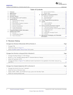
Table of Contents
1 Features.......................................................................... 1
2 Applications................................................................... 1
3 Description..................................................................... 1
4 Revision History........................................................... 2
5 Pin Configuration and Functions.............................. 3
6 Specifications................................................................ 4
6.1 Absolute Maximum Ratings.................................... 4
6.2 ESD Ratings............................................................ 5
6.3 Recommended Operating Conditions................. 5
6.4 Thermal Information............................................... 5
6.5 Electrical Characteristics....................................... 6
6.6 Timing Characteristics......................................... 10
6.7 Typical Characteristics........................................ 10
7 Parameter Measurement Information.................. 12
8 Detailed Description.................................................. 13
8.1 Overview................................................................ 13
8.2 Functional Block Diagram................................... 14
8.3 Feature Description.............................................. 15
8.4 Device Functional Modes.................................... 16
8.5 Register Maps....................................................... 22
9 Application and Implementation............................. 28
9.1 Application Information....................................... 28
9.2 Typical Applications............................................ 28
9.3 System Examples.................................................. 36
10 Power Supply Recommendations......................... 37
11 Layout........................................................................... 38
11.1 Layout Guidelines............................................... 38
11.2 Layout Example................................................... 39
12 Device and Documentation Support..................... 40
12.1 Third-Party Products Disclaimer....................... 40
12.2 Receiving Notification of Documentation Updates 40 12.3 Support Resources 40
12.4 Trademarks......................................................... 40
12.5 Electrostatic Discharge Caution........................ 40
12.6 Glossary.............................................................. 40
13 Mechanical, Pacjaging, and Orderable Information 40
![]()
4 Revision History
Changes from Revision B (November 2018) to Revision C Page
• Changed Title............................................................................................................................................................................................. 1
• Added Description for Figure 18.......................................................................................................................................................... 28
•
Added Simplified System without Power Path section.................................................................................................................... 35
Changes from Revision A (August 2014) to Revision B Page
• Changed Handling Ratings To: ESD Ratings..................................................................................................................................... 5
• Moved Tstg From: Handling Ratings table To: Absolute Maximum Ratings................................................................................... 5
• Added the Application NOTE................................................................................................................................................................ 28
• Changed the Notes to Figure 27 for additional resistor requirement to the application circuit when using low VGS
input FETs................................................................................................................................................................................................ 37
Changes from Original (September 2011) to Revision A Page
• Changed the format to the new TI standard........................................................................................................................................ 1
• Added the Device Information table...................................................................................................................................................... 1
• Added LODRV, HIDRV, and PHASE (2% duty cycle) to the Abs Max Table................................................................................. 4
•
Added the Handling Ratings table......................................................................................................................................................... 5

![]()
![]()
![]()
![]()
![]() ACN ACP CMSRC ACDRV
ACOK
ACN ACP CMSRC ACDRV
ACOK
LODRV GND SRP SRN BATDRV
Pin Functions
|
PIN |
DESCRIPTION |
|
|
NO. |
NAME |
|
|
1 |
ACN |
Input current sense resistor negative input. Place an optional 0.1µF ceramic capacitor from ACN to GND for common- mode filtering. Place a 0.1µF ceramic capacitor from ACN to ACP to provide differential mode filtering. |
|
2 |
ACP |
Input current sense resistor positive input. Place a 0.1µF ceramic capacitor from ACP to GND for common-mode filtering. Place a 0.1µF ceramic capacitor from ACN to ACP to provide differential-mode filtering. |
|
3 |
CMSRC |
ACDRV charge pump source input. Place a 4kΩ resistor from CMSRC to the common source of ACFET (Q1) and RBFET (Q2) limits the in-rush current on CMSRC pin. |
|
4 |
ACDRV |
Charge pump output to drive both adapter input n-channel MOSFET (ACFET) and reverse blocking n-channel MOSFET (RBFET). ACDRV voltage is 6V above CMSRC when voltage on ACDET pin is between 2.4V to 3.15V, voltage on VCC pin is above UVLO and voltage on VCC pin is 275mV above voltage on SRN pin so that ACFET and RBFET can be turned on to power the system by AC adapter. Place a 4kΩ resistor from ACDRV to the gate of ACFET and RBFET limits the in-rush current on ACDRV pin. |
|
5 |
ACOK |
AC adapter detection open drain output. It is pulled HIGH to external pull-up supply rail by external pull-up resistor when voltage on ACDET pin is between 2.4V and 3.15V, and voltage on VCC is above UVLO and voltage on VCC pin is 275mV above voltage on SRN pin, indicating a valid adapter is present to start charge. If any one of the above conditions can not meet, it is pulled LOW to GND by internal MOSFET. Connect a 10kΩ pull up resistor from ACOK to the pull-up supply rail. |
|
6 |
ACDET |
Adapter detection input. Program adapter valid input threshold by connecting a resistor divider from adapter input to ACDET pin to GND pin. When ACDET pin is above 0.6V and VCC is above UVLO, REGN LDO is present, ACOK comparator and IOUT are both active. |
|
7 |
IOUT |
Buffered adapter or charge current output, selectable with SMBus command ChargeOption(). IOUT voltage is 20 times the differential voltage across sense resistor. Place a 100pF or less ceramic decoupling capacitor from IOUT pin to GND. |
|
8 |
SDA |
SMBus open-drain data I/O. Connect to SMBus data line from the host controller or smart battery. Connect a 10kΩ pull- up resistor according to SMBus specifications. |
|
9 |
SCL |
SMBus open-drain clock input. Connect to SMBus clock line from the host controller or smart battery. Connect a 10kΩ pull-up resistor according to SMBus specifications. |
|
10 |
ILIM |
Charge current limit input. Program ILIM voltage by connecting a resistor divider from system reference 3.3V rail to ILIM pin to GND pin. The lower of ILIM voltage or DAC limit voltage sets charge current regulation limit. To disable the control on ILIM, set ILIM above 1.6V. Once voltage on ILIM pin falls below 75mV, charge is disabled. Charge is enabled when ILIM pin rises above 105mV. |
|
11 |
BATDRV |
Charge pump output to drive Battery to System n-channel MOSFET (BATFET). BATDRV voltage is 6V above SRN to turn on BATFET to power the system from battery. BATDRV voltage is SRN voltage to turn off BATFET to power system from AC adapter. Place a 4kΩ resistor from BATDRV to the gate of BATFET limits the in-rush current on BATDRV pin. |
Pin Functions (continued)
|
PIN |
DESCRIPTION |
|
|
NO. |
NAME |
|
|
12 |
SRN |
Charge current sense resistor negative input. SRN pin is for battery voltage sensing as well. Connect SRN pin to a 7.5 Ω resistor first then from resistor another terminal connect a 0.1µF ceramic capacitor to GND for common-mode filtering and connect to current sensing resistor. Connect a 0.1µF ceramic capacitor between current sensing resistor to provide differential mode filtering. See application information about negative output voltage protection for hard shorts on battery to ground or battery reverse connection by adding small resistor. |
|
13 |
SRP |
Charge current sense resistor positive input. Connect SRP pin to a 10 Ω resistor first then from resistor another terminal connect to current sensing resistor. Connect a 0.1µF ceramic capacitor between current sensing resistor to provide differential mode filtering. See application information about negative output voltage protection for hard shorts on battery to ground or battery reverse connection by adding small resistor. |
|
14 |
GND |
IC ground. On PCB layout, connect to analog ground plane, and only connect to power ground plane through the power pad underneath IC. |
|
15 |
LODRV |
Low side power MOSFET driver output. Connect to low side n-channel MOSFET gate. |
|
16 |
REGN |
Linear regulator output. REGN is the output of the 6V linear regulator supplied from VCC. The LDO is active when voltage on ACDET pin is above 0.6V and voltage on VCC is above UVLO. Connect a 1µF ceramic capacitor from REGN to GND. |
|
17 |
BTST |
High side power MOSFET driver power supply. Connect a 0.047µF capacitor from BTST to PHASE, and a bootstrap Schottky diode from REGN to BTST. |
|
18 |
HIDRV |
High side power MOSFET driver output. Connect to the high side n-channel MOSFET gate. |
|
19 |
PHASE |
High side power MOSFET driver source. Connect to the source of the high side n-channel MOSFET. |
|
20 |
VCC |
Input supply, diode OR from adapter or battery voltage. Use 10Ω resistor and 1µF capacitor to ground as low pass filter to limit inrush current. |
|
PowerPAD™ |
Exposed pad beneath the IC. Analog ground and power ground star-connected only at the PowerPAD plane. Always solder PowerPad to the board, and have vias on the PowerPAD plane connecting to analog ground and power ground planes. It also serves as a thermal pad to dissipate the heat. |
|
6 Specifications
6.1 Absolute Maximum Ratings
over operating free-air temperature range (unless otherwise noted)(1) (2)
|
|
MIN MAX |
UNIT |
|
|
|
SRN, SRP, ACN, ACP, CMSRC, VCC |
–0.3 30 |
|
|
|
PHASE |
–2 30 |
|
|
|
ACDET, SDA, SCL, LODRV, REGN, IOUT, ILIM, ACOK |
–0.3 7 |
|
|
Voltage range |
BTST, HIDRV, ACDRV, BATDRV |
–0.3 36 |
|
|
|
–4 7 |
V |
|
|
|
HIDVR (2% duty cycle) |
–4 36 |
|
|
|
PHASE (2% duty cycle) |
–4 30 |
|
|
Maximum difference |
SRP–SRN, ACP–ACN |
–0.5 0.5 |
|
|
voltage |
|
|
|
|
Junction temperature range, TJ |
–40 155 |
°C |
|
|
Storage temperature range, Tstg |
–55 155 |
°C |
|
(1) Stresses beyond those listed under absolute maximum ratings may cause permanent damage to the device. These are stress ratings only, and functional operation of the device at these or any other conditions beyond those indicated under recommended operating conditions is not implied. Exposure to absolute-maximum-rated conditions for extended periods may affect device reliability.
(2) All voltages are with respect to GND if not specified. Currents are positive into, negative out of the specified terminal. Consult Packaging Section of the data book for thermal limitations and considerations of packages.
6.2 ESD Ratings
|
|
VALUE |
UNIT |
||
|
V(ESD) |
Electrostatic discharge |
Human body model (HBM), per ANSI/ESDA/JEDEC JS-001, all pins(1) |
±2000 |
V |
|
Charged device model (CDM), per JEDEC specification JESD22-C101, all pins(2) |
±500 |
|||
(1) JEDEC document JEP155 states that 500-V HBM allows safe manufacturing with a standard ESD control process.
(2) JEDEC document JEP157 states that 250-V CDM allows safe manufacturing with a standard ESD control process.
6.3 Recommended Operating Conditions
over operating free-air temperature range (unless otherwise noted)
|
|
MIN |
NOM |
MAX |
UNIT |
|
|
Voltage range |
SRN, SRP, ACN, ACP, CMSRC, VCC |
0 |
24 |
V |
|
|
PHASE |
-2 |
24 |
|||
|
ACDET, SDA, SCL, LODRV, REGN, IOUT, ILIM, ACOK |
0 |
6.5 |
|||
|
BTST, HIDRV, ACDRV, BATDRV |
0 |
30 |
|||
|
Maximum difference voltage |
SRP–SRN, ACP–ACN |
–0.2 |
0.2 |
V |
|
|
Junction temperature range, TJ |
0 |
125 |
°C |
||
6.4 Thermal Information
|
THERMAL METRIC(1) |
BQ24725A |
UNIT |
|
|
RGR [VQFN] |
|||
|
20 PIN |
|||
|
RθJA |
Junction-to-ambient thermal resistance |
46.8 |
°C/W |
|
RθJCtop |
Junction-to-case (top) thermal resistance |
56.9 |
|
|
RθJB |
Junction-to-board thermal resistance |
46.6 |
|
|
ψJT |
Junction-to-top characterization parameter |
0.6 |
|
|
ψJB |
Junction-to-board characterization parameter |
15.3 |
|
|
RθJCbot |
Junction-to-case (bottom) thermal resistanc |
4.4 |
|
(1) For more information about traditional and new thermal metrics, see the Semiconductor and IC Package Thermal Metrics application report.


Tidak ada komentar:
Posting Komentar